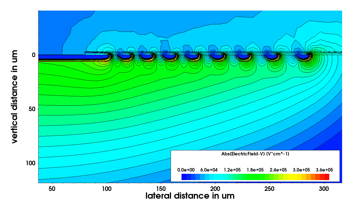
Termination Design
The junction termination is a key part of every power semiconductor device. It has a major impact on both device reliability and electrical performance.
We have extensive experience in the design of reliable, compact, and manufacturable termination structures across a wide range of technologies and voltage classes.
Modern power devices are expected to meet demanding reliability requirements, including humidity stress tests such as HV-H3TRB. Our termination concepts have consistently demonstrated outstanding robustness, passing these tests without degradation well beyond the 1,000-hour requirement specified by industry standards.
In addition to ensuring long-term reliability, our designs minimize termination area, maximizing the available active chip area and thereby contributing to lower conduction losses and improved overall device performance.
Services
Engineering, optimization, and qualification for all common termination concepts including:
- Floating Field Rings, primarily used for lower-voltage devices
- Variation of Lateral Doping (VLD) terminations for high-voltage applications
- Ring-Assisted VLD structures, widely adopted in SiC power devices
Automated Termination Design Algorithm
The video below demonstrates our fully automated termination design algorithm generating a 1200V ring termination. Depending on the available simulation resources, a complete and optimized 1200V termination design can be generated overnight, eliminating the need for time-consuming manual optimization.
The result is a faster development cycle, reduced engineering effort, and highly optimized termination structures with predictable performance.